Tanushree H. Choudhury
Tanushree H. Choudhury
tanuhc[at]iitb[dot]ac[dot]in
(+91) (022) 2576 7610
Assistant Professor
View profile

Tanushree H. Choudhury
tanuhc[at]iitb[dot]ac[dot]in
(+91) (022) 2576 7610
Assistant Professor
Associate Professor
Avradeep Pal
Email: avradeep[at]iitb[dot]ac[dot]in
Phone: (+91) (022) 2576 7629
Education:
In his teaching, Avradeep focuses primarily on conceptual understanding of origin of physical phenomena, with a special attention to stay clear of rote memorisation as much as possible. Courses taught: Undergraduate Structure of Materials Post Graduate Advanced Ceramics (Piezoelectrics, Ferromagnets, Superconductors)
Avradeep's interests lie in the sphere of development, understanding and utilisation of novel phenomena that arises at hybrid material interfaces, and development of several novel quantum devices. The major focus is on the interface of thin film superconductors and ferromagnets. His work therefore spans from controlled Ultra High Vacuum growth of ultra thin film (2nm and lower) multilayers, to nanofabrication of these layers into devices like tunnel junctions, spin valves, Jospehson junctions; and subsequent low temperature electronic transport measurements of such devices. For achieving the same, he has developed several highly customised UHV thin film deposition and fabrication systems, and has standardised a industry level niobium based junction fabrication process. This has led to the discovery of novel cryogenic memory devices and other cryogenic components such as Josephson diodes that are crucial for upcoming era of quantum technologies.
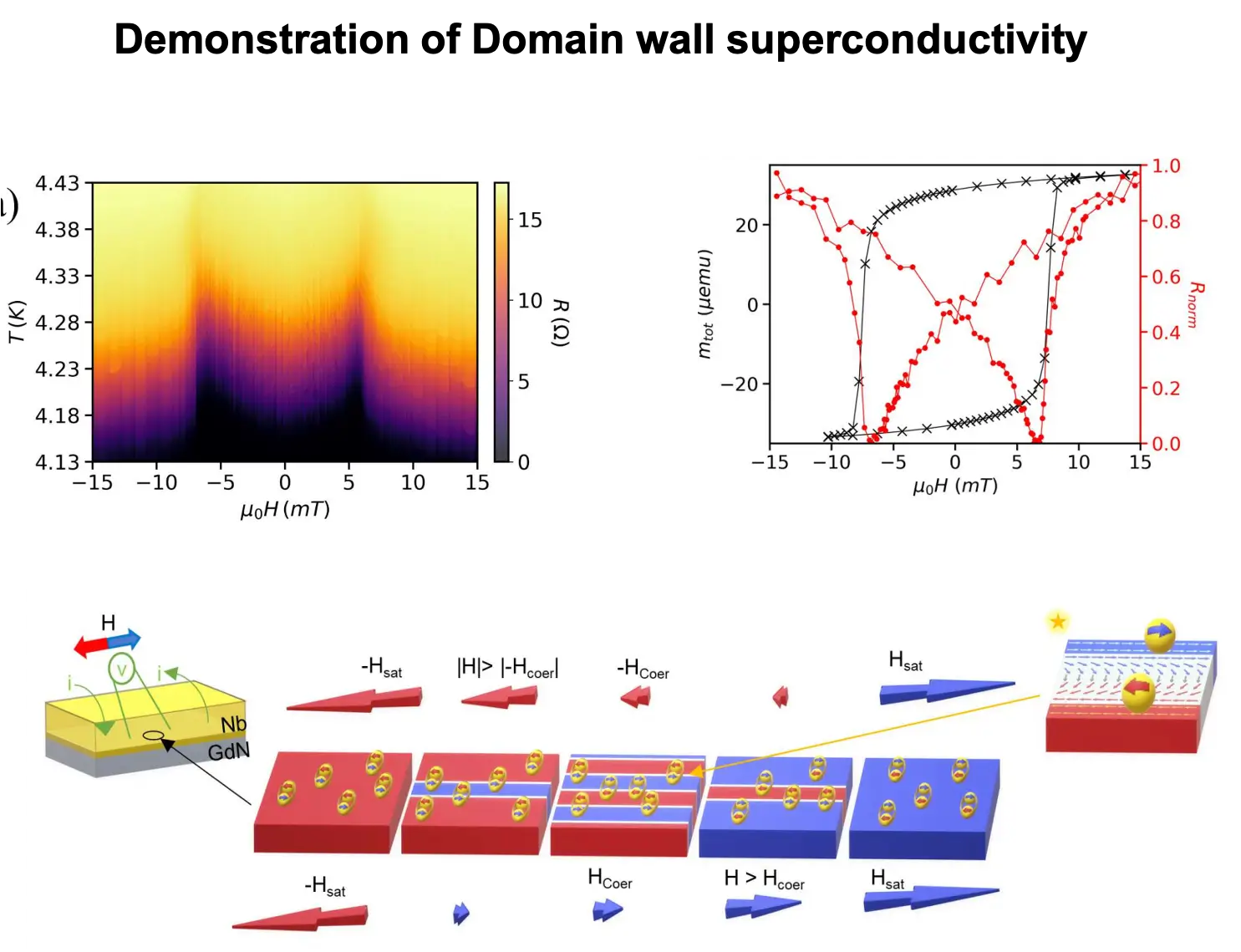
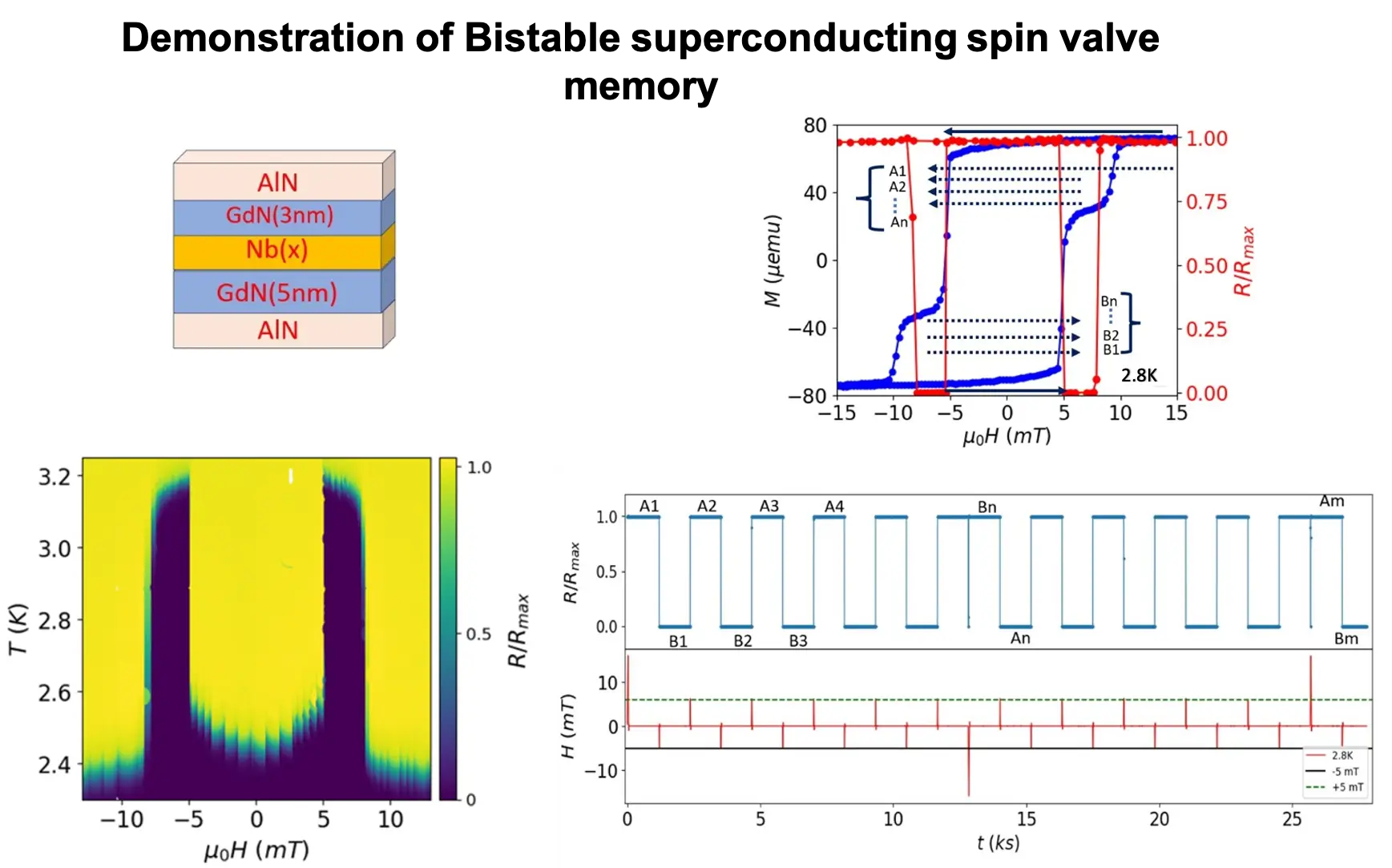
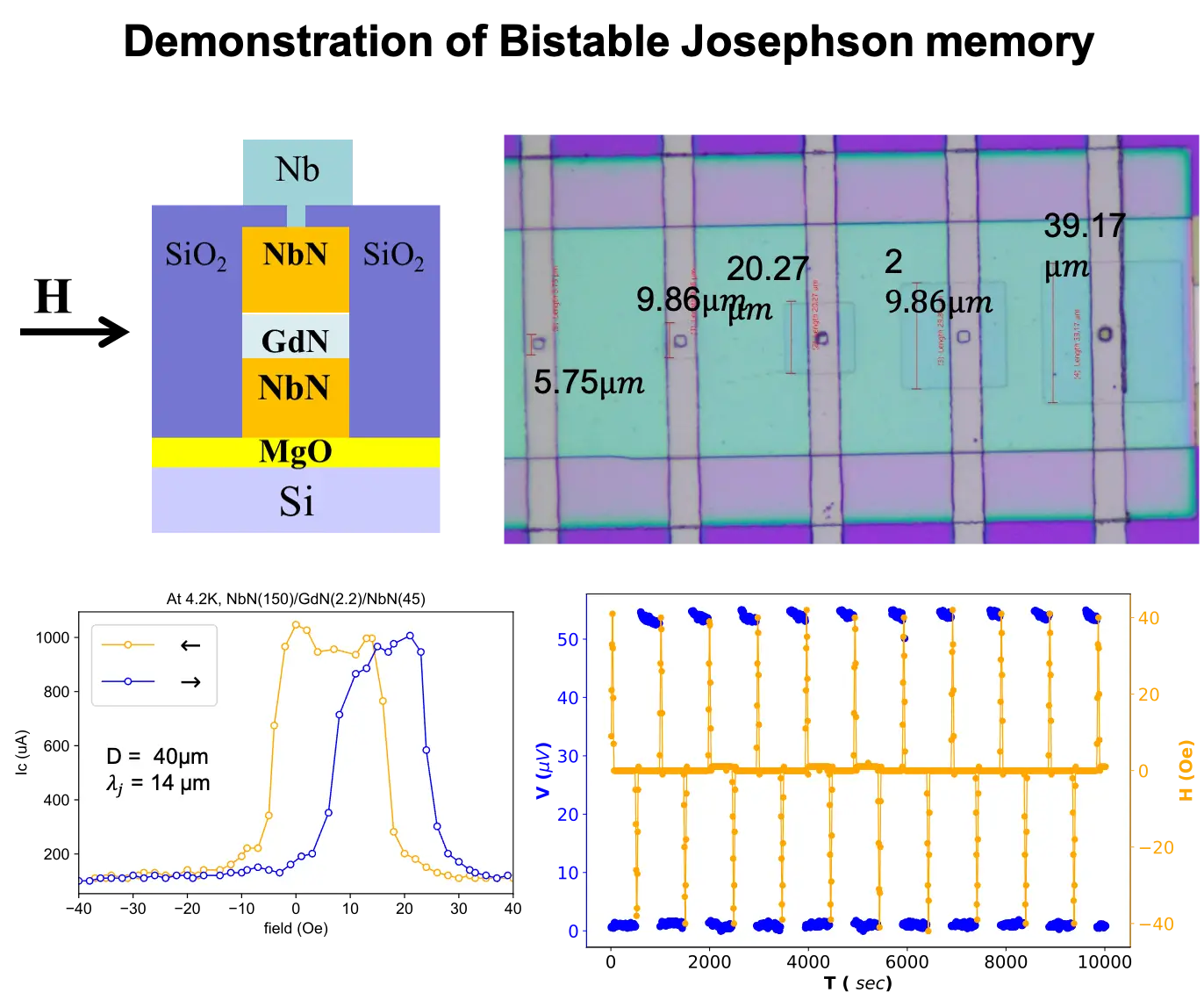
Domain wall superconductivity in GdN/Nb bilayers
Superconducting exchange coupling driven memory device
High frequency Josephson memory device at 4.2K
Professor
Amartya Mukhopadhyay
Email: amartya_mukhopadhyay[at]iitb[dot]ac[dot]in
Phone: (+91) (022) 2576 7612
Education:
Teaches undergraduate courses on 'Electrochemistry of Materials and its Applications', 'Advanced Ceramics', 'Advanced Composites', postgraduate course on 'Structural Characterization of Materials'; have designed an elective course on 'Electrochemical and Materials Perspectives in Energy Storage'
Prof Amartya Mukhopadhyay completed his Doctoral in Materials Research from the University of Oxford, UK, in 2009. He did his postdoctoral Research at Brown University, USA, for a couple of years. He is a Young Associate of the Indian National Academy of Engineering (INAE) and served as the Honorary Secretary of Mumbai Chapter of the Indian Institute of Metals (IIM). His research interests include materials for electrochemical energy storage (focusing on alkali metalion batteries) and engineering ceramics. Among his major accomplishments, he has been awarded with the ‘SwarnaJayanti Fellowship 202021’, recognized by the Royal Society of Chemistry (UK) journals as one of the ‘2019 Emerging Investigators’, awarded with the 'IIT Bombay Research Dissemination Award 2018', 'INAE Young Engineer Award 2016', 'ASMIIM North America Visiting Lectureship 2016', 'IIT Bombay Young Investigator Award 2014' and 'Dr. R. L. Thakur Memorial Award' by the 'Indian Ceramic Society' in 2013.
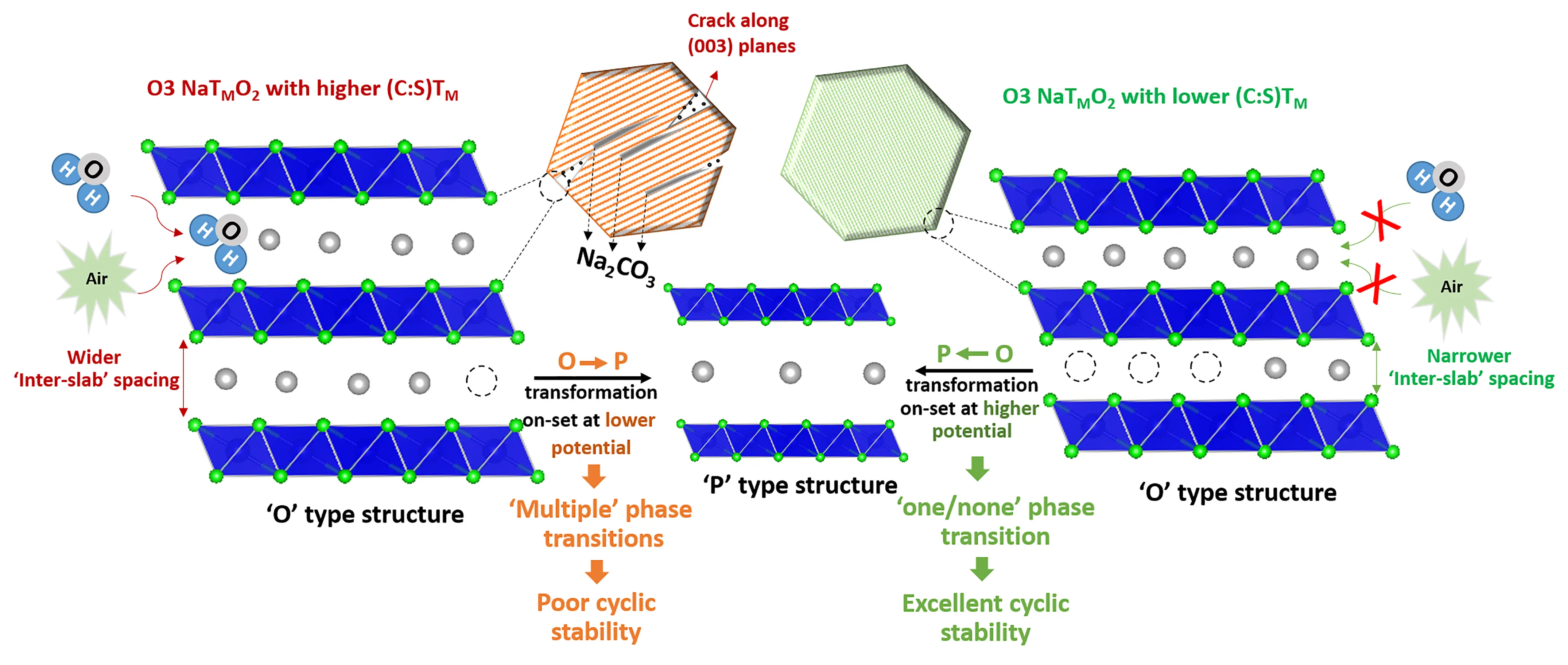
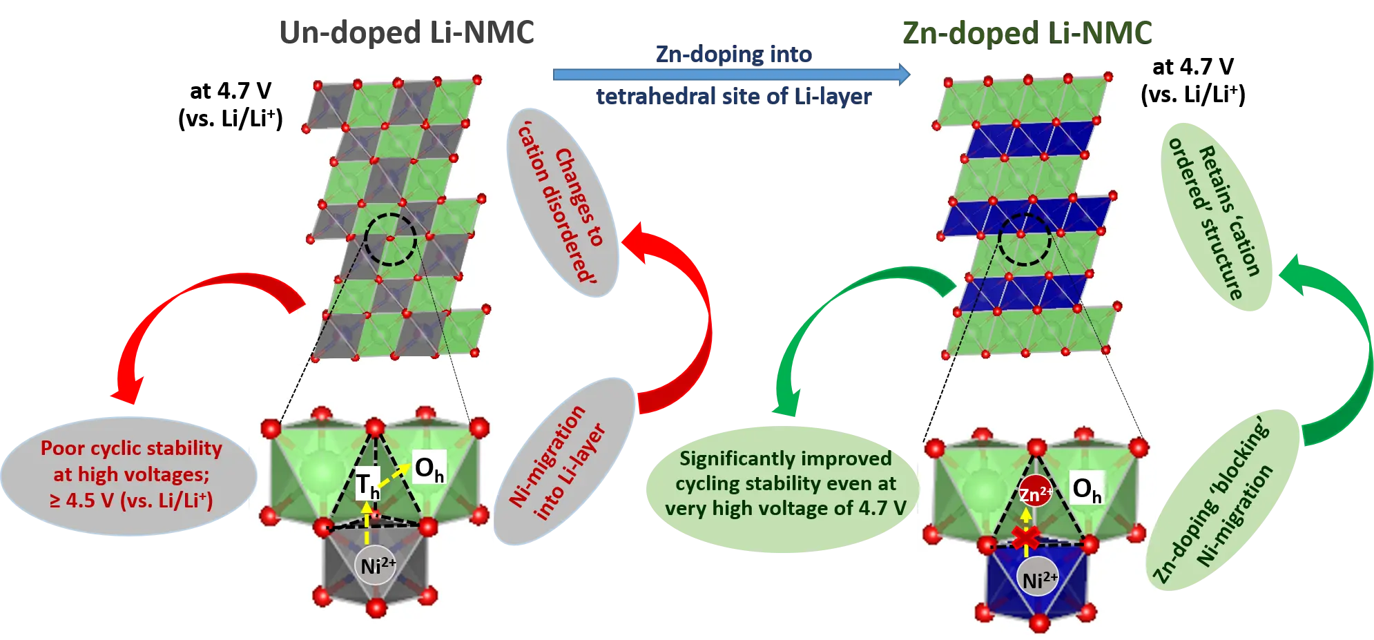
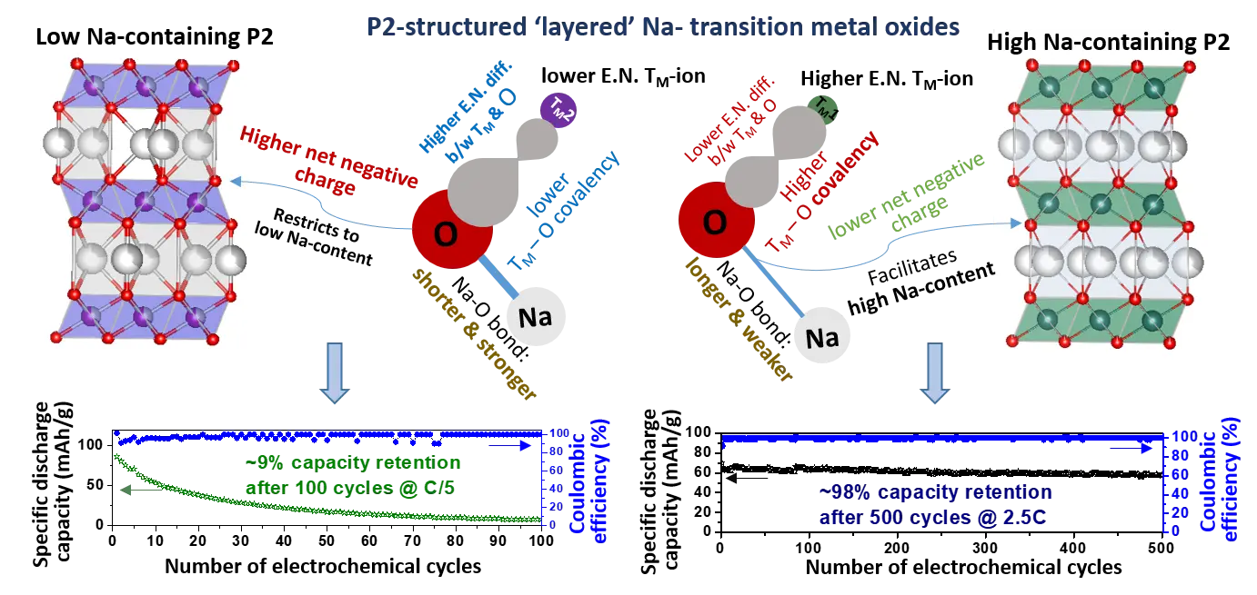
Revealing the dominant factors/parameters towards addressing air/water- instability and structural- cum electrochemical instability of ‘layered’ Na- tran sition metal oxide based cathode materials for Naion
Addressing High Voltage Structural and Electrochemical Instability of Nicontaining Layered Transition Metal (TM) Oxide cathodes by ‘blocking’ the ‘TMmigration’ pathway in the Lattice [2]
Designing high Na- containing P2structured ‘layered’ Na transition metal oxides as high- performance cathode materials for Naion batteries [3]
Assistant Professor
Abhinandan Gangopadhyay
Email: abhinandan[dot]g[at]iitb[dot]ac[dot]in
Phone: (+91) (022) 2576 7603
Education:
Prof. Gangopadhyay has taught undergraduate course on Mechanical Behaviour of Materials. He will be offering a comprehensive graduate level course on Transmission Electron microscopy.
Prof. Abhinandan Gangopadhyay is interested in applying advanced electron microscopy techniques to study defects and interfaces in advanced functional and structural materials. He has previously studied the core structure of various interfacial defects such as dissociated 60° dislocation [1], Lomer dislocation [2], dissociated 90° dislocation [3] in GaAs(001)based heterostructures using highangle annulardarkfield (HAADF) mode of aberrationcorrected scanning transmission electron microscopy (ACSTEM). Prof. Gangopadhyay has also worked on STEMEDX characterization of grain boundary segregation in novel polycrystalline GaInP solar cells. As part of his recent industrial work experience, he has worked on nanometerscale characterization of stateoftheart semiconductor devices using focused ion beam (FIB) technique in conjunction with ACSTEM. His current research interests include segregation studies using STEM spectrum images and strain mapping using geometric phase analysis (GPA) and 4D STEM in advanced materials.
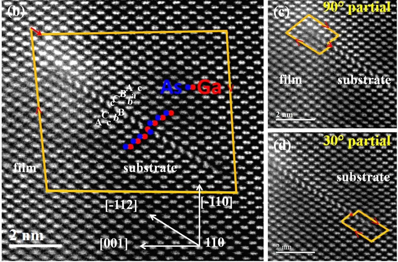
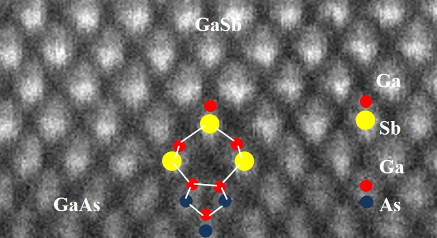
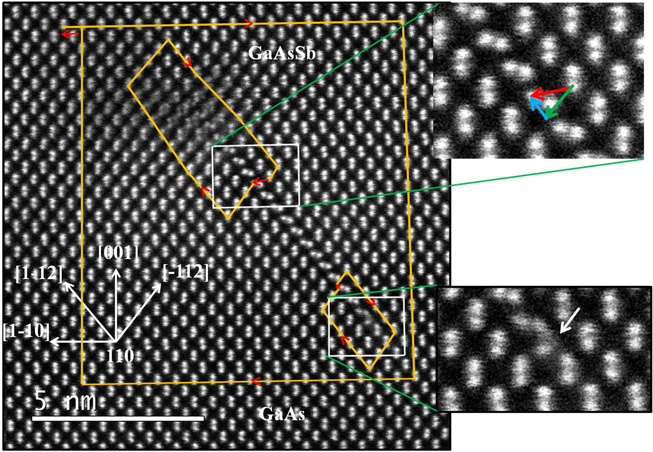
Aberrationcorrected HAADFSTEM images of dissociated 60 degree dislocation and its bounding partials located at GaAsSb/GaAs interface [1]
Aberrationcorrected HAADFSTEM image of a Lomer dislocation located at GaSb/GaAs interface [2]
Aberrationcorrected HAADFSTEM image of a dissociated 90 degree dislocation located at GaAsSb/GaAs interface [3]
Assistant Professor
Abhijeet L. Sangle
Email: alsangle[at]iit[dot]ac[dot]in
Phone: (+91) (022) 2159 6742
Education:
Abhijeet is interested in pedagogy of structureproperty relationships and functional materials in general.
UG courses: Structure of Materials (Autumn semester), Materials Processing Laboratory (Spring semester)
PG courses: Principles and Applications of Ferroelectric and Piezoelectric materials (proposed, starting Spring semester 2024)
Abhijeet works in the broad area of thin films of functional materials for various applications. He is particularly interested in employing nanostructuring to enhance various properties of thin films of functional materials. One of the main themes of his research is selfassembled vertically aligned nanocomposite (VAN) films incorporating functional materials such as piezoelectrics, ferroelectrics, thermoelectrics and photoactive materials for applications in the areas of tunable high frequency devices 1 , sensors and actuators; energy harvesting 2 and storage; nonvolatile memories 3 , etc. Abhijeet leverages the pulsed laser deposition facilities available in the department to grow these films. Besides, he is also working towards building a multitarget co- sputter deposition facility equipped with advanced in situ diagnostics. Drawing inspiration from his prior work in aerosoljet printing technology 4 , Abhijeet is also working on developing bespoke inks of functional materials for various printed electronic devices. In the past, Abhijeet was a part of the corporate R & D division of Applied Materials India, where he worked on large area deposition of thin films of various piezoelectric materials. Given his background in industry, Abhijeet is highly passionate about translational research, taking labscale ideas to working prototypes/scaling up studies.
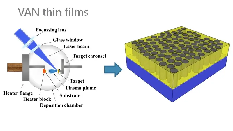
Schematic of PLD and VAN th in films
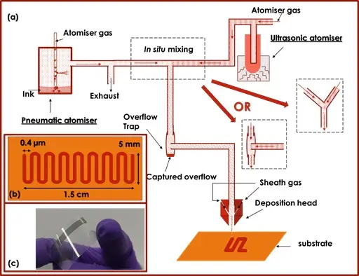
Schematic of Aerosoljet printing process showing implementation of in situ mixing to print composite materials
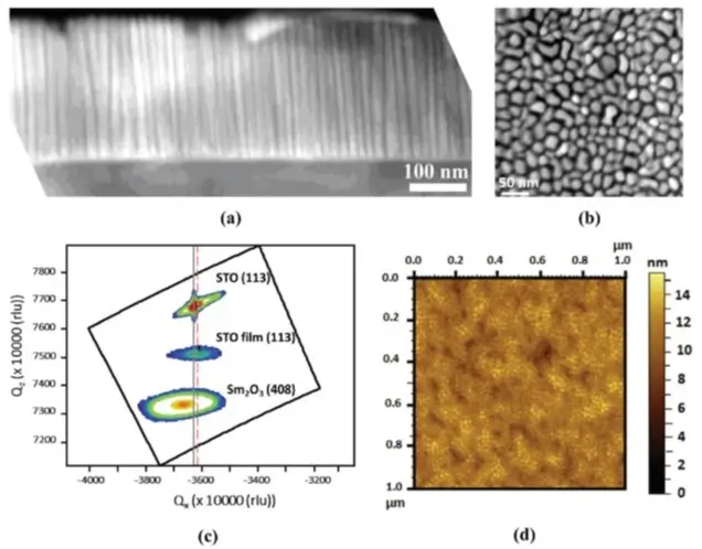
SrTiO3Sm2O3 (3070 wt%) VAN films, 250nm thick (a) Crosssectional STEM, (b) Plan- view STEM, (c) reciprocal space map, (d) AFM image showing topography. Source: Sangle, A. L., et al., Nanoscale (2018); STEM image credits: H. Wang group, TAMU (now at Purdue)
Avradeep Pal
avradeep[at]iitb[dot]ac[dot]in
(+91) (022) 2576 7629
Associate Professor
Amartya Mukhopadhyay
amartya_mukhopadhyay[at]iitb[dot]ac[dot]in
(+91) (022) 2576 7612
Professor
Abhinandan Gangopadhyay
abhinandan[dot]g[at]iitb[dot]ac[dot]in
(+91) (022) 2576 7603
Assistant Professor
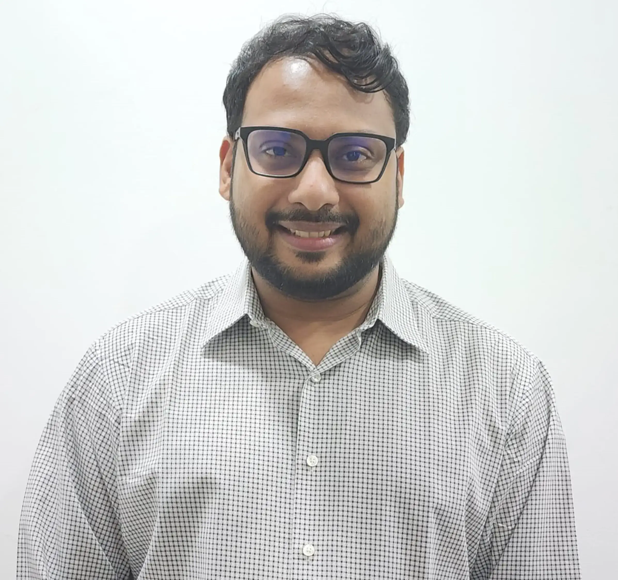
Abhijeet L. Sangle
alsangle[at]iitb[dot]ac[dot]in
(+91) (022) 2159 6742
Assistant Professor