

Assistant Professor
Tanushree H. Choudhury
Email: tanuhc[at]iitb[dot]ac[dot]in
Phone: (+91) (022) 2576 7610
Education:
- PhDMaterials Research Centre, IISc, Bangalore, 2014;
- MSc, Materials Science Anna University, Chennai 2007
In her teaching, Prof. Tanushree H. Choudhury gives special emphasis on correlating optoelectronic properties of materials with applications.
A few courses taught by her are as follows:
Undergraduate courses: Electronic properties of mate rials, Sensors and Measurements lab
Postgraduate course: Electrical materials: fundamentals to applications
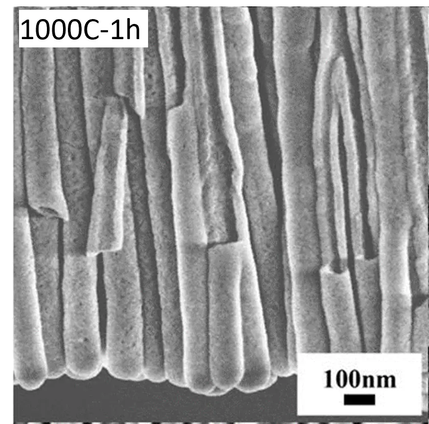
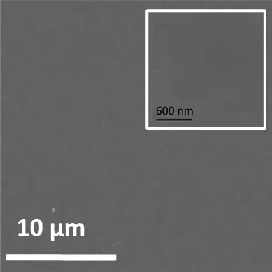
Prof. Tanushree Choudhury is interested in the processing of electronic materials for optoelectronic applications. She has experience with waferscale synthesis of ‘nearsingle crystal’ epitaxial layered transition metal dichalcogenides by metalorganic chemical vapor deposition (MOCVD). The key to achieving epitaxial coalesced films was controlling the surface termination of the sapphire substrate.[1,2] The nucleation and growth stages were separated out to achieve larger domains and lower grain boundaries. She is extending this work by introducing defects and modulating composition of these monolayer epitaxial films. She has also been involved in the synthesis of anodized oxide nanostructures on films and as freestanding membranes, where solution treatment can be used to increase the thermal stability of these nanostructures.[3] These anodized nanostructures are ideal candidates for sensing and capacitive deionization. Her group is now exploring the synthesis of airstable layered materials by solution synthesis which can be used for low power transistors and neuromorphic applications. By controlling the solvent, ambient for crystallization and the nucleation rates, coalesced films of layered molybdenum oxide have been synthesized. Controlling the nucleation rates and suppressing diffusion of species is key to achieving coalesced films of these materials. These coalesced oxide films can now serve as substrates as will used as independent optoelectronic elements. Her research focusses on establishing the processing property correlation while emphasizing on the mechanism for the microstructure formation.
- Layered semiconductor synthesis Nanostructure synthesis
- Wafer scale semiconductor thin film synthesis Processproperty correlation for optoelectronics
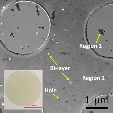
Waferscale WS2 grown by MOCVD
Anodized nanostructured zirconia after 1000C treatment
Coalesced MoO3 films synthesized by solution synthesis
- Choudhury, T.H., Zhu, H., Nayir, N., et al. Step engineering for nucleation and domain orientation control in WSe2 epitaxy on cplane sapphire. Nat. Nanotechnol. (2023).
- Choudhury, T.H., Chubarov, M., WaferScale Epitaxial Growth of Unidirectional WS2 Monolayers on Sapphire. ACS Nano, 15, 2, 2532–2541(2021) Anodized nanostructured zirconia after 1000C treatment
- Choudhury, T.H. et al. Chemically enhanced thermal stability of anodized nanostructured zirconia membranes, J. Mater. Chem., 22, 68856893 (2012)