

Triratna P. Muneshwar
Email: tmuneshwar[at]iitb[dot]ac[dot]in
Phone:(+91) (022) 2576 7640
Education:
- B.Tech and M.Tech (Dual Degree), MEMS, IIT Bombay 2009
- PhD Chemical and Materials Engineering, University of Alberta, 2014
In his teaching, Prof. Muneshwar uses examples from range applications (like modern electronics, biology, sensors, etc) for students to appreciate the underlying fundamental materials science processes.
Some of the courses taught are:
Undergraduate Courses: Kinetics of Processes, Semiconductor Devices and Processing
Postgraduate Courses: Experiments Vacuum Thin film Materials Processing Lab
Prof. Triratna P Muneshwar's research interests are in the development of thin film deposition and etching processes for applications in modern semiconductor devices, flexible electronics, Modification of interface layers in fuelcells and battery. He uses fundamental understanding of the involved steps (precursor/byproduct transport under vacuum, surface reactions, surface diffusion, etc,) for rapid development of the novel deposition/etching processes and making existing processes more efficient.
- Metal and Semiconducting Materials for logic/memory device applications Modelling of vacuum processes for thin film deposition and etching
- Atomic Layer Deposition and Atomic Layer Etching (ALD/ALE)
- LabtoFab ALD/ALE process solutions
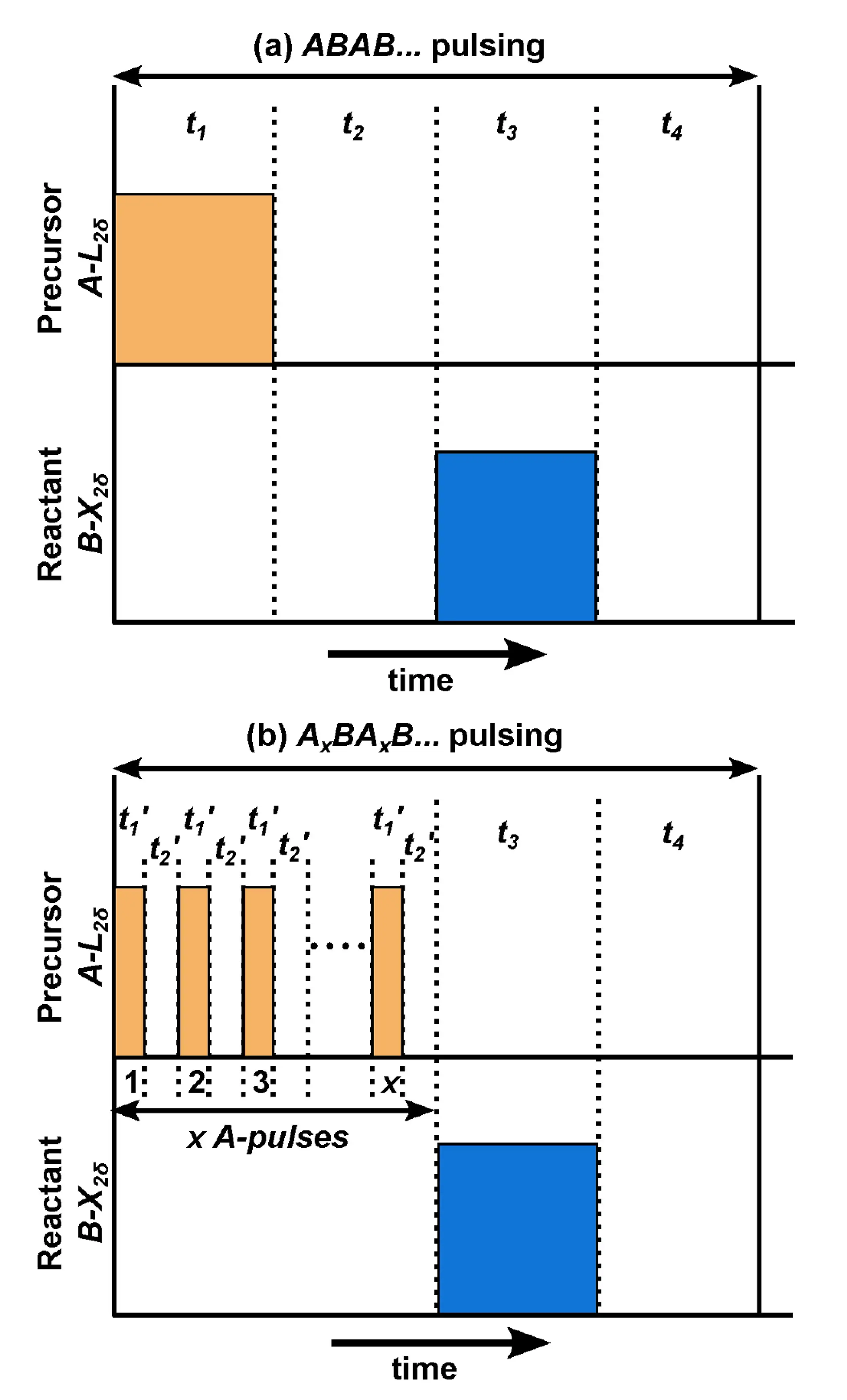
Micropulsing using AxBAxB... sequence against conventional ABAB... sequence for high throughput ALD processes
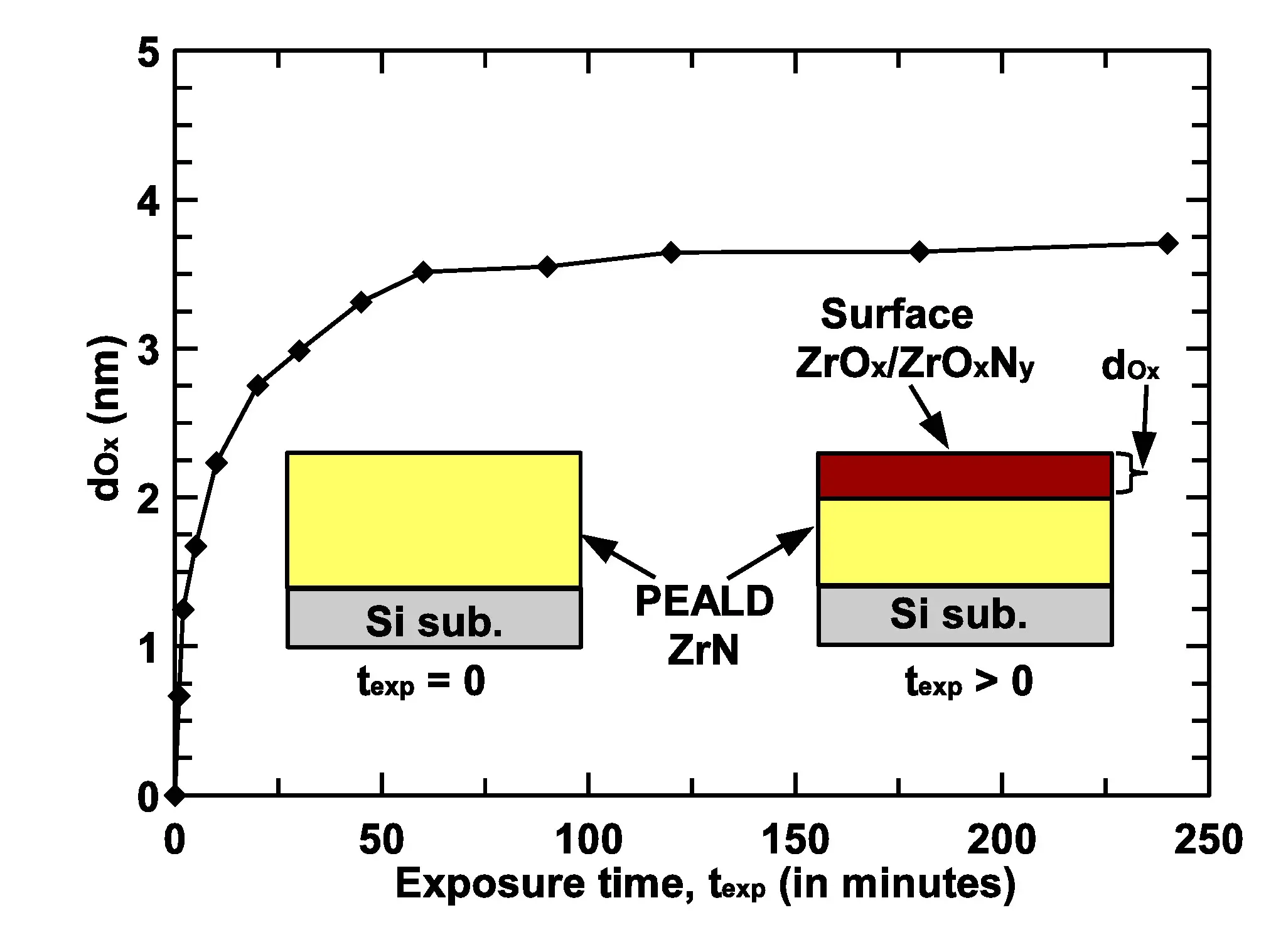
Thickness of surface oxide (dOx) on bare ZrN PEALD film against ambient exposure time (texp) using spectroscopic ellipsometry measurements. ZrN films grown at 150 °C were cooled under vacuum before ambient exposure.
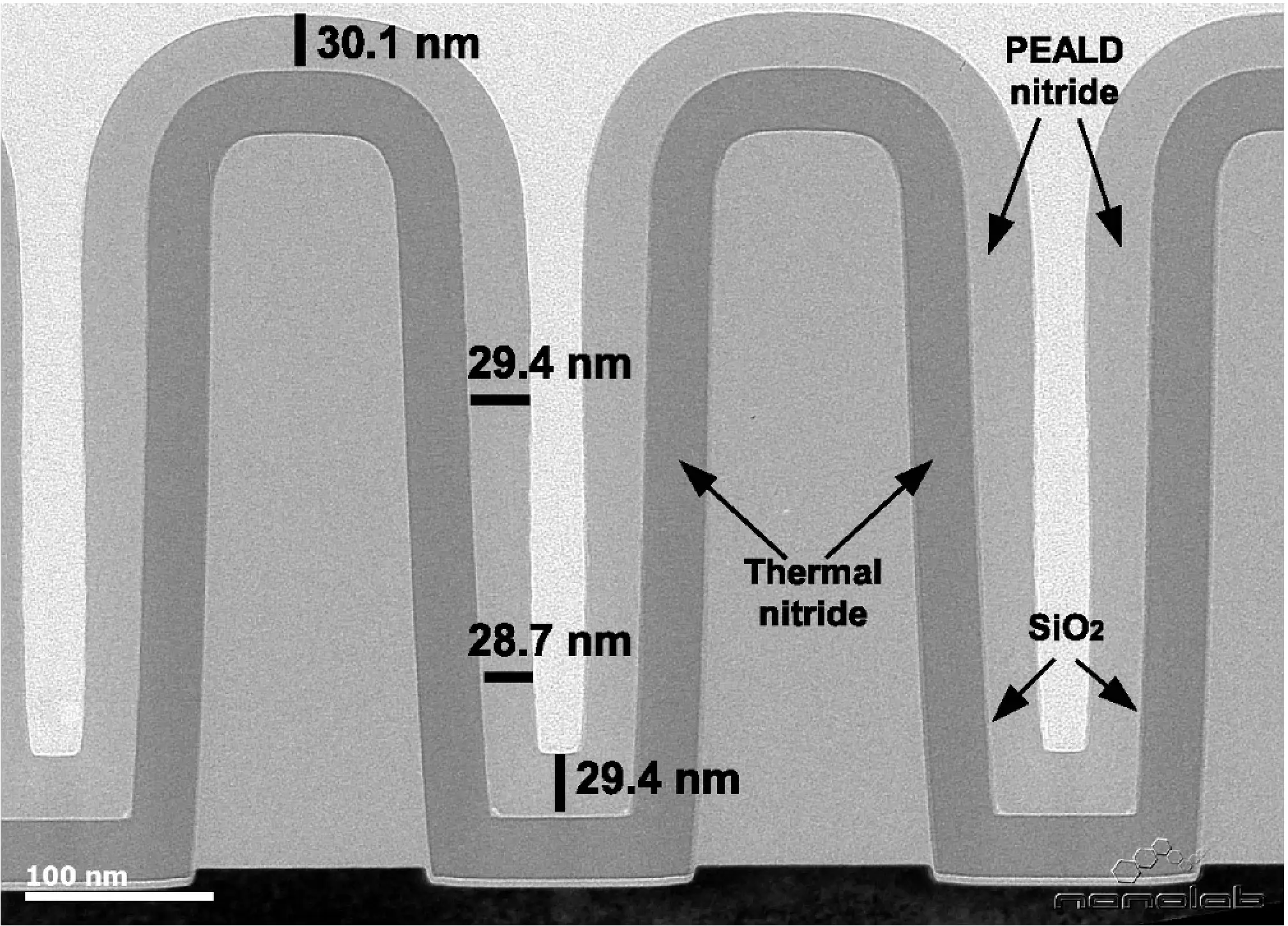
Crosssectional TEM image of SiNx PEALD film deposited at 100 °C, showing a sidewall step coverage > 95% in a trench structure of aspect ratio 4.5.
- T. Muneshwar, K. Cadien, AxBAxB... pulsed atomic layer deposition: Numerical growth model and experiments, J. Appl. Phys. 119 (2016) 085306) [1]
- T. Muneshwar, K. Cadien, Comparing XPS on bare and capped ZrN films grown by plasma enhanced ALD: Effect of ambient oxidation, App. Surf. Sci. 435, (2018) 367376) [2]
- T. Muneshwar, K. Cadien, Resolving selflimiting growth in silicon nitride plasma enhanced atomic layer deposition with trisdimethylamino silane precursor, J. Vac. Sci. Technol. A. 38 (2020) 062406) [3]